
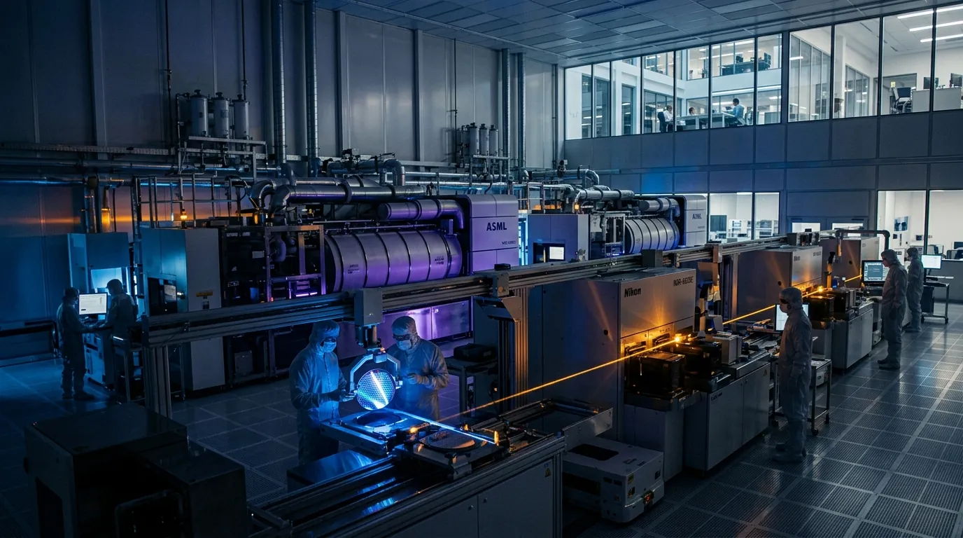
Rooted in the philosophy of "Design • Innovate • Deliver", Power Silicon Technologies Pvt. Ltd. is an engineering-first semiconductor house dedicated to VLSI excellence and embedded integration.
Power Silicon (Power Silicon Technologies Pvt. Ltd.) is a premier Indian semiconductor engineering company headquartered in Hyderabad & Bengaluru, India. We deliver end-to-end VLSI architecture, custom ASIC/SoC micro-architecture, UVM verification, 2nm/3nm physical design signoff, analog layout, and embedded firmware.
With core engineering resources focused on Digital VLSI Design, Advanced Verification, and Physical Signoff, we partner with global fabless semiconductor companies, Tier-1 automotive OEMs, and hyper-scale innovators to tape out complex SoCs and ASICs on time with first-pass silicon precision.
Our dedicated Embedded Systems practice ensures that your silicon comes alive immediately with production-grade Board Support Packages (BSPs), device drivers, and post-silicon validation routines.
To be the trusted semiconductor design execution partner for the world's most critical compute, automotive, and artificial intelligence silicon.
To eliminate silicon risk and compress tape-out timelines through extreme verification depth, architectural rigor, and transparent engineering collaboration.
Every project at Power Silicon Technologies is governed by four immutable engineering commitments.
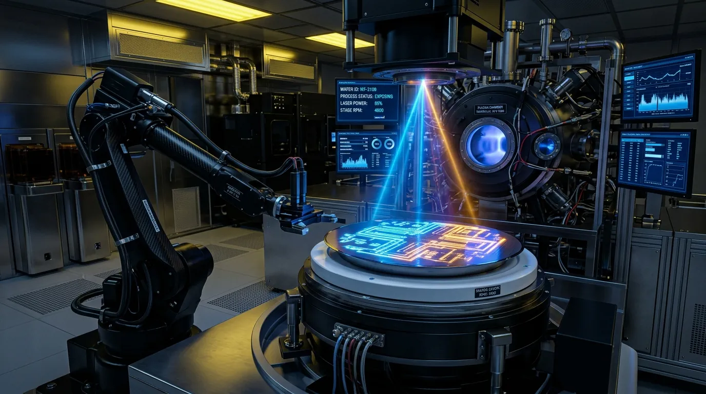 Principle 01
No shortcuts. We enforce exhaustive linting, CDC/RDC checks, and 100% formal and functional coverage closure before signoff.
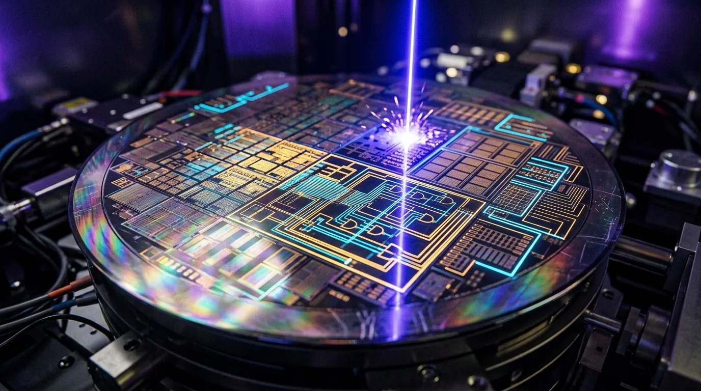 Principle 02
Tape-out respins cost millions. Our multi-corner STA signoff and silicon validation checklists guarantee first-pass functionality.
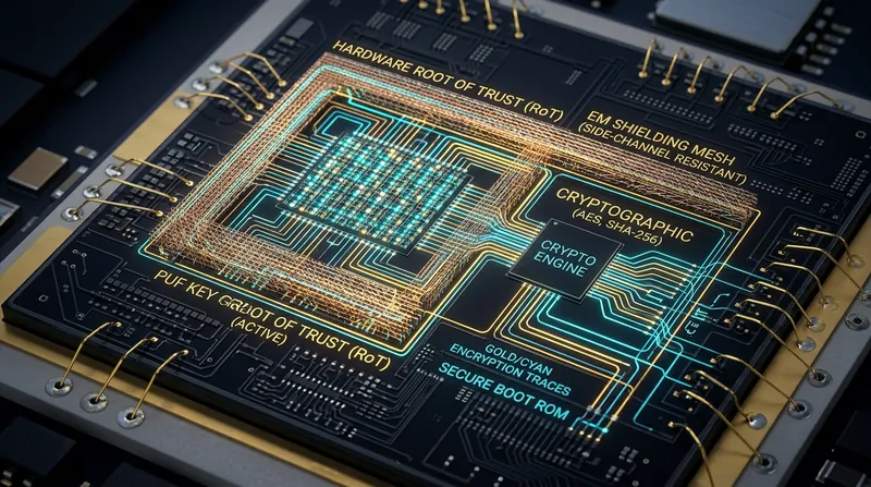 Principle 03
Complete client data segregation with military-grade network security, encrypted design servers, and robust legal NDA frameworks.
 Principle 04
From full turnkey design ownership to targeted ODC staff augmentation, we adapt seamlessly to your engineering pipeline.
We seamlessly plug into your existing EDA workflows and foundry design environments.