
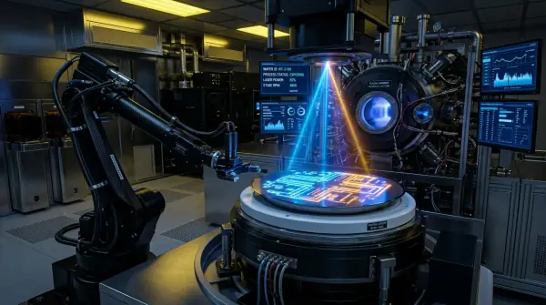
We specialize in end-to-end VLSI design and physical implementation, enabling complex SoCs and IPs from RTL through signoff and tapeout with a focus on performance, power, area, and quality.
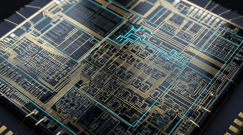 VLSI RTL Design
Micro-architecture definition, high-performance Verilog/SystemVerilog RTL coding, SoC integration, and low-power UPF/CPF.
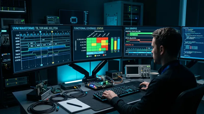 Design & Verification
Constrained-random verification with SystemVerilog/UVM, Formal property checking, gate-level simulation (GLS), and coverage closure.
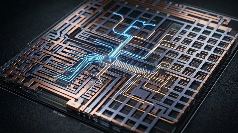 Physical Design
Complete backend flow: Netlist-to-GDSII, hierarchical floorplanning, Clock Tree Synthesis (CTS), STA timing, and DRC/LVS closure.
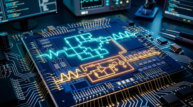 Analog Design
Transistor-level schematic design, high-speed PLLs, ADCs/DACs, bandgaps, low-dropout regulators (LDOs), and mixed-signal AMS co-simulation.
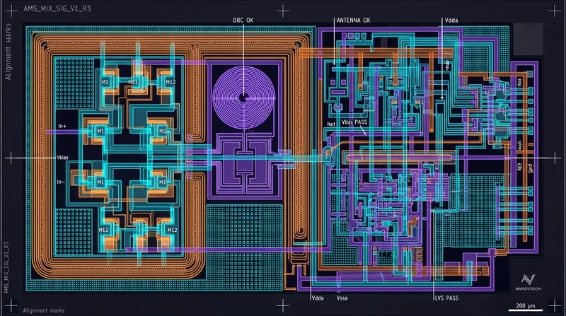 Analog Layout
Precision custom IC layout, matching strategies (common centroid), guard ringing, noise isolation, and full DRC/LVS/ERC signoff.
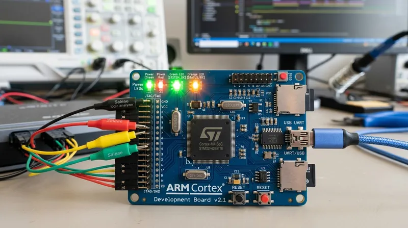 Embedded Systems
Essential board bring-up, Linux & FreeRTOS Board Support Packages (BSP), bare-metal firmware, peripheral drivers, and validation.
Our structured silicon engineering lifecycle ensures predictable execution, first-pass tape-out success, and flawless embedded enablement.
System specification, PPA budgeting (Power, Performance, Area), and IP selection.
Modular Verilog/SystemVerilog design, bus interconnects, and UPF low-power intent.
Constrained-random testbenches, assertions, coverage metrics, and formal verification.
Hierarchical floorplanning, placement, clock tree synthesis (CTS), and routing.
Multi-corner STA, DRC/LVS verification, IR drop analysis, and GDSII foundry release.
Post-silicon validation, BSP driver development, and hardware-software integration.
Power Silicon Technologies engineers operate natively within Tier-1 commercial EDA environments from Synopsys, Cadence, and Siemens EDA. We support leading semiconductor foundry design kits (PDKs) across TSMC, Intel Foundry Services, Samsung, and GlobalFoundries.
Synopsys PrimeTime & Fusion Compiler, Cadence Innovus, Siemens Calibre (DRC/LVS/PEX), and Ansys RedHawk-SC (IR Drop & EM).
Experience spanning 28nm, 16nm/12nm FinFET, 7nm, 5nm, down to cutting-edge 3nm and 2nm.
We combine the agility of a specialized boutique team with the rigorous execution standards of premier semiconductor design houses.
No middle layers or diluted priorities. Every project is staffed with senior VLSI and firmware specialists dedicated to technical precision.
Bank-grade data isolation, encrypted remote design environments, strict NDAs, and full intellectual property ownership retained by you.
Pre-built verification VIP modules, proven tape-out checklists, and concurrent firmware bring-up reduce tape-out schedules by up to 30%.
Leading the semiconductor design wave with turnkey ASIC development, advanced physical signoff down to 2nm, and mission-critical embedded systems engineering.
Power Silicon (Power Silicon Technologies Pvt. Ltd.) is an Indian semiconductor engineering and custom ASIC/SoC design company headquartered in Hyderabad & Bengaluru, India. We deliver end-to-end VLSI architecture, RTL micro-architecture, UVM verification, 2nm/3nm physical design signoff, analog layout, and embedded firmware.
Power Silicon is a dedicated B2B semiconductor and custom chip design engineering firm based in India. It is completely independent and distinct from consumer flash memory storage brand Silicon Power (SP) and general power semiconductor electronic components.
Our headquarters and advanced VLSI design center are located in Hyderabad, Telangana, with an active engineering presence across Bengaluru, Karnataka, delivering silicon solutions to clients in India, North America, Europe, and Asia.
We offer turnkey milestone SOWs, Offshore Dedicated Centers (ODCs), and task-force team augmentation. Contact our VLSI Principal Architects via our RFQ Portal or reach us directly on WhatsApp at +91 94931 36675.