

We deliver end-to-end semiconductor lifecycle services specializing in advanced VLSI Design, Verification, and Physical Signoff alongside Embedded Systems Enablement.
End-to-end semiconductor capabilities across digital, analog mixed-signal, backend physical signoff, and embedded enablement.
 VLSI RTL Design
Micro-architecture definition, high-performance Verilog/SystemVerilog RTL coding, SoC integration, and low-power UPF/CPF.
 Design & Verification
Constrained-random verification with SystemVerilog/UVM, Formal property checking, gate-level simulation (GLS), and coverage closure.
 Physical Design
Complete backend flow: Netlist-to-GDSII, hierarchical floorplanning, Clock Tree Synthesis (CTS), STA timing, and DRC/LVS closure.
 Analog Design
Transistor-level schematic design, high-speed PLLs, ADCs/DACs, bandgaps, low-dropout regulators (LDOs), and mixed-signal AMS co-simulation.
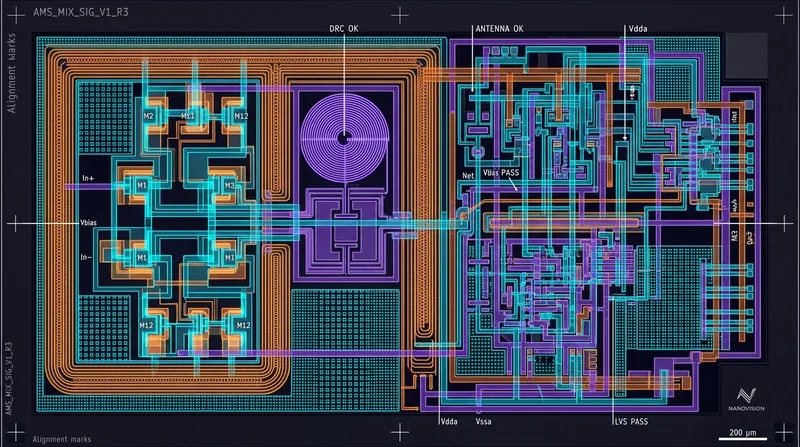 Analog Layout
Precision custom IC layout, matching strategies (common centroid), guard ringing, noise isolation, and full DRC/LVS/ERC signoff.
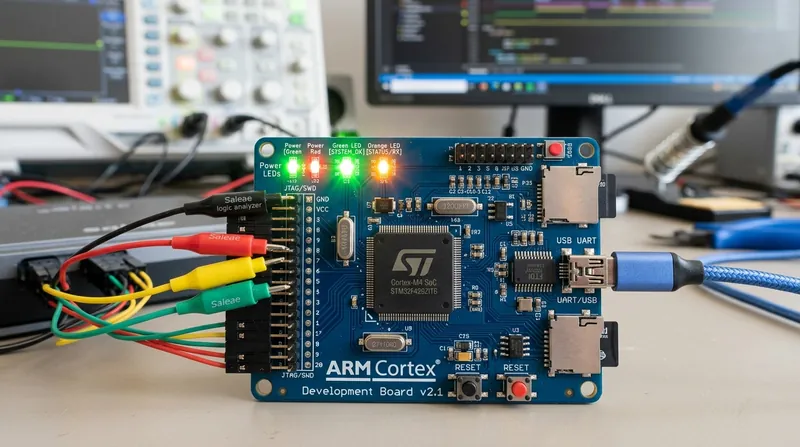 Embedded Systems
Essential board bring-up, Linux & FreeRTOS Board Support Packages (BSP), bare-metal firmware, peripheral drivers, and validation.
Choose the operational model that matches your product roadmap and engineering bandwidth.
End-to-end milestone-based delivery from spec to GDSII signoff. We take full ownership of schedules, EDA tooling, and tape-out deliverables.
Augment your in-house team with senior RTL, DV, Physical Design, or Embedded engineers who integrate directly into your Git/EDA flows.
Targeted execution for specific high-risk bottlenecks such as timing closure crunch, formal verification signoff, or complex power optimization.